From fungible computing to silicon photonics, including neuromorphic computing, an overview of the techniques that are shaping the future of high-performance computing.
Semiconductors have become one of the sinews of the AI war. The JDN looked into their future by examining the most promising avenues for development.
The GPU optimization stack or AI as an ecosystem
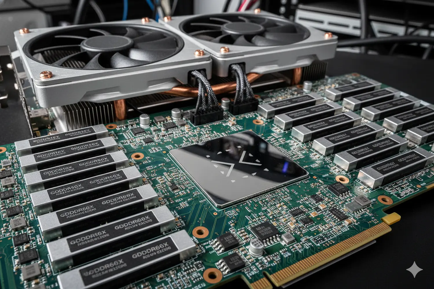
Set of software and hardware layers which make it possible to optimize the computing power of a GPU, the optimization stack makes it possible to minimize the resources consumed by AI, at a time when the cost of the token becomes, as Jensen Huang has affirmed during Nvidia’s annual conference, a major issue.
It includes the entire AI value chain, from raw silicon to final application. It is therefore a question of optimizing both the hardware (GPU architecture, memory bandwidth, number of cores) as well as the drivers (which provide the interface between the operating system and the hardware, like the CUDA programming platform at Nvidia), the libraries written by chip manufacturers and optimized for their hardware (cuDNN for deep learning, TensorRT for inference), or even deep learning frameworks. (PyTorch, TensorFlow).
For Ian Cutress, CEO of More than Moore, an analyst firm specializing in semiconductors, it is Nvidia’s ability to think across the entire stack that explains its overwhelming dominance in the AI market, more than the power of its graphics processing units (GPUs).
“CUDA is not just a programming language, it is a complete ecosystem of libraries, tools familiar to developers, kernels optimized deployment flows and low-level settings. “Today, GPUs are no longer sold solely on FLOPS, but more importantly on customers’ ability to actually extract performance, deploy models, debug systems, and scale across entire clusters.”
If Nvidia is ahead, its competitors have taken note and are also developing their own ecosystem. “AMD is making progress in this area with ROCm, while other vendors leverage the open ecosystem of frameworks like PyTorch, TensorFlow, and platforms like Hugging Face.”
Fungible computing or interchangeable computing resources
Fungible compute is an IT infrastructure concept which is based on the idea of making computing resources (processors, memory, storage, network) interchangeable, shared and dynamically allocable, rather than fixed and dedicated to a particular machine or use.
From Google to Nvidia, via Oracle, the AI giants currently growing this concept within their data centers, in order to completely rethink their infrastructure to optimize the energy efficiency of AI and easily adapt to new uses.
“We are completely redefining cloud infrastructure,” Pradeep Vincent, senior vice president and chief technical architect of Oracle Cloud Infrastructure, said recently. Microsoft, one of the three cloud giants along with Amazon and Google, recently acquired Fungible, specifically with this in mind. This young company uses a type of microprocessor called a data processing unit (DPU), with low energy consumption. According to the company, this technology helps improve the efficiency of calculations in server nodes, as well as the exchange of data between these nodes. Microsoft thus intends to make the infrastructure of its data centers more efficient, scalable, disaggregated and deployed on a large scale, while being reliable and secure.
In San Francisco, the start-up Decart, which allows AI developers to easily alternate between processors from Nvidia, Amazon, Google and others, reached a valuation of 4 billion dollars after an investment round in which Nvidia put 300 million.
Let us also cite the young company NextSilicon, an Israeli start-up whose Maverick-2 chip uses a dataflow architecture which reprograms itself in real time depending on the type of calculation in progress. “The company seeks to overcome the traditional divide between CPU and GPU by executing calculations as close as possible to the structure of the program itself, rather than passing everything through a conventional flow of instructions,” explains Ian Cutress.
Silicon photonics
This technology consists, as its name suggests, of integrating optical components (waveguide, signal modulator, photodetector, etc.) on a silicon chip. Unlike a traditional chip, information circulates in the form of photons on silicon and not electrons on copper wires. Light allows much larger volumes of data to be transmitted with less energy.
The technology is actually not that new: in the 1980s, researchers began to propose placing circuits designed for photons on the same chip as circuits designed for electrons, and in the early 2000s, Intel carries out pioneering research in this matter. But it is the rise of AI which is giving a real boost to this technology, by making the volume of data transmitted/energy ratio particularly strategic. “Moving data electrically is becoming too expensive in terms of range and energy consumption,” says Ian Cutress.
At the beginning of March, European STMicroelectronics announced the large-scale production of its cutting-edge PIC100 platform based on silicon photonics. “Looking to the future, we are planning and implementing capacity increases to enable more than four-fold production growth by 2027. This rapid ramp-up relies entirely on our customers’ long-term capacity reservation commitments,” Fabio Gualandris, President of Quality, Manufacturing & Technology at STMicroelectronics, said at the time.
The giants Samsung, TSMC, AMD, as well as the young shoots Ayar Labs, which raised 500 million dollars in early March, and Lightmatter, in which invest hyperscalers are also active in this area.
“This technology is highly strategic, as AI systems are increasingly limited by the efficiency with which GPUs, memory, switches and racks can communicate with each other. Progress is substantial, with optical chiplets, co-packaged optics and photonic interposers now moving from research to product roadmaps. The largest clusters are expected to move there in the near term, while copper will remain dominant in much of the market,” estimates Ian Cutress.
Neuromorphic computing
This is undoubtedly the most revolutionary approach among all the innovations cited in this article, since it involves nothing more and nothing less than rethinking the fundamental architecture of chips by implementing an alternative to Von Neumann’s architecture which equips all our current computers. To do this, neuromorphic computing is inspired by the functioning of the human brain, through artificial neurons and synapses.
“The next generation of AI and hyperscale computing requires a move away from traditional Von Neumann architecture in favor of new designs that prioritize the balance between raw performance, extreme energy efficiency and architectural flexibility,” said Mina Kim, principal economist at MKEcon Insights, a research and business intelligence platform.
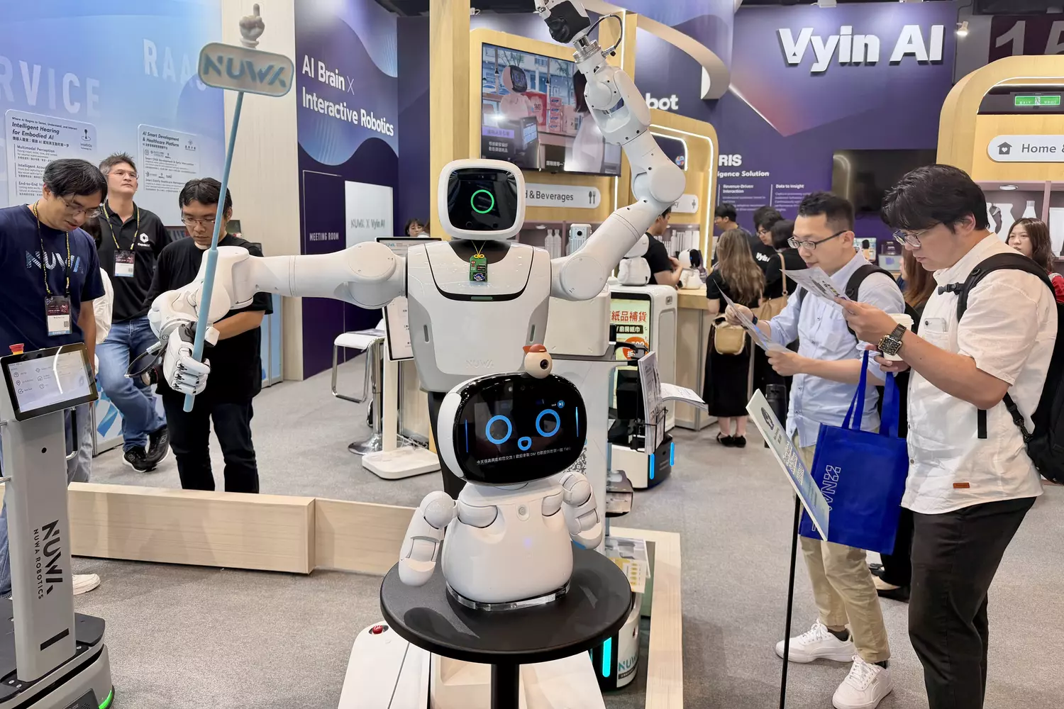
In addition to the prospect of greater energy efficiency and lower latency, this new architecture is seen as strategic for cutting-edge uses, such as robotics, embedded AI and adaptive learning.
For Ian Cutress, it is not intended to replace GPUs, the two ecosystems are rather destined to coexist. “I would describe it more as a long-term, specialized architecture that could become important where event data and ultra-low power consumption are paramount.” Intel is particularly active in this area, with its chip Loihi 2. Let us also cite IBM with TrueNorth, and the start-up BrainChip with its Akida chip, or even INRIA in France.