Announced during the Choose France summit, the new factory that the group is building in partnership with Radiall and the Taiwanese Foxconn responds to a crucial link in the semiconductor value chain: advanced packaging.
At the beginning of June, the European Commission presented its version 2.0 of the Chips Actaiming to strengthen European autonomy in semiconductors, based on the model of what the United States has been doing since 2022 with their own Chips Act. At the same time, Thalès, Foxconn and Radiall took a concrete step in this direction: a joint investment of 250 million euros for the construction of a packaging factory for semiconductors in France.
Europe today produces around 10% of the semiconductors used in the world, compared to 25% in 2000. But this general figure hides disparities in the types of chips. Europe is, for example, absent from the production of high-end chips dedicated to AI, the manufacturing of which is heavily concentrated in Taiwan. On the other hand, it is very present, notably via France and Germany, in the production of power semiconductors and chips for industry, automobiles, railways and aeronautics, thanks to champions like Infineon, NXP and STMicroelectronics.
Missing niches in the value chain
These divergences are also visible at different levels of the value chain. For example, Europe is very powerful in the equipment used to manufacture cutting-edge chips, thanks to the Dutch company ASML. This is the only global manufacturer of EUV (extreme ultraviolet radiation lithography) machines, essential for producing chips with an engraving fineness of less than 7 nm, used by AI giants.
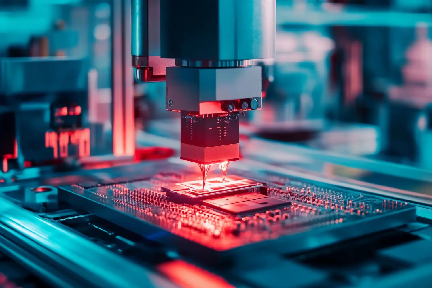
On the other hand, Europe is very weak in foundry activities enabling these chips to be manufactured, but also in packaging, the next step. Once this chip has been manufactured, it must be molded into a housing to make it a component that can be transferred to a printed circuit. This is the role of packagers, also called OSAT, for Outsourced Semiconductor Assembly and Test, specialized in chip assembly and testing. This activity is today largely concentrated in Asia, in Taiwan, but also in China, Malaysia and Thailand.
It is this missing niche that Thalès, Foxconn and Radiall intend to fill through their Tessalia factory project, announced at the Choose France summit and which is due to open in the Bordeaux region in 2029. In particular, the objective is to specialize in Systems in Package, or SIP, multi-chip packages which consist of an advanced packaging technique, targeting the mid- and high-end markets. If the technique was invented by two European research institutes, the Fraunhofer-Gesellschaft in Germany and the CEA-Leti in France, the industrial know-how was delocalized to Asia in the 1990s and no longer exists on the Old Continent.
Rebuilding an integrated subsidiary in Europe
The objective of the project is to regain this capacity on European soil. “In Europe, we know how to make prototypes, but not produce on an industrial scale. However, microelectronics relies a lot on know-how, factory and process adjustment, machine adjustment, which this project will make it possible to acquire via a technology transfer from Foxconn to Europe,” explains Damien Jugie, head of the Tessalia joint venture for Thalès.
The joint venture therefore aims to pool the industrial strength of Thalès, the know-how and strategic market position of Foxconn, as well as Radiall’s experience in the manufacturing of cutting-edge components for electronics. “Foxconn is the third private employer in the world and the first EMS, it manufactures everything related to hardware for Sony or Apple, and has, among other things, a production agreement with NVIDIA. France has a very rich ecosystem of suppliers of equipment for processing chips, cutting machines, thinning machines, etc. Our observation is that all the pieces of the ecosystem are in place, what is simply missing is a catalyst that will make it possible to unite this entire ecosystem around a single project. We hope Tessalia will be that catalyst.”
Production at the Tessalia factory will be dedicated in part to the supercomputer market, but also to components for sensors or radio-frequency systems, intended in particular for telecoms infrastructures, as well as various industrial markets (automobile, medical, robotics, aeronautics, space and defense). If the company is not yet communicating the identity of its partners in the European semiconductor market, it claims to have the ambition to source its AI chips in Europe and not in Asia, which would probably involve sourcing from the factories that Intel and TSMC are building in Germany. “The idea is of course to use European foundries, and to carry out the packaging in Europe to have a verticalized European offer”, summarizes Damien Jugie.
Gaining strength in the European market
The advantage of a factory specialized in packaging is that it costs much less than a foundry designed for the manufacture of AI chips, the cost of which today amounts to several tens of billions of dollars. This is mainly due to the difference in the fineness of the engraving (less than 7 nanometers for an AI chip, where Tessalia aims for track widths of the order of 1 to 10 microns, one micron equivalent to 1,000 nanometers). The finer it is, the more the clean room must be under control: protection against dust, management of humidity, vibrations and magnetic fields.
In the most high-end clean rooms, a simple connected watch is prohibited, because it generates a magnetic field likely to influence the engravings and therefore ruin the quality of the wafers. They are also forced to compensate for the movements of the moon. The Tessalia factory does not face such constraints, even if the three companies still chose a largely isolated location to avoid, for example, the vibrations linked to the passage of cars on the highway.
The objective is to produce 100,000 wafers per year in 2032, which gives around 60 million components, given that there are 600 SIPs per wafer. With the objective of increasing to 250,000 wafers in 2038. “The advanced packaging market in Europe today represents around 2% of the global market. Europe is therefore almost non-existent. Tessalia’s ambition is to capture between 15 and 20% of the European market share”, notes Damien Jugie.
According to him, the factory relies on several innovative production processes to achieve its objective. “In this factory, the substrate will be produced with a semiconductor process rather than a potential printed circuit process, which will allow us to be ten times denser and above all to have higher yields. Then, these components will be able to accommodate very heterogeneous functions, therefore digital functions, optoelectronic functions, power functions, RF functions, in the same component. This modularity of functions is also possible thanks to metal deposition capabilities to avoid radiation, in the service of greater versatility of components.
Finally, we will be able to mold the entire component, mark it and single it out to deliver it to the customer. These components will be smaller, lighter and less consuming than current components, providing access to new product architectures. In a word, we are setting up a whole flow of innovation around industrial production processes to gain efficiency, competitiveness and of course independence.”